Moore’s Law vs. Metrology: The Role of Measurement in Pushing Optical Limits with Erik Hosler

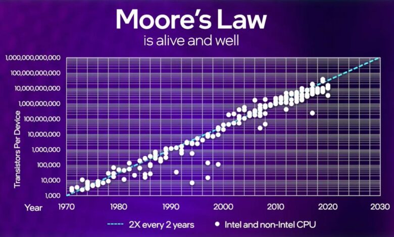
For decades, Moore’s Law served as the guiding principle of semiconductor progress, promising a doubling of transistor density every two years. But as features shrink to the atomic scale and architectures grow more complex, one overlooked element may become the ultimate arbiter of progress: measurement. In today’s manufacturing environment, the ability to precisely monitor and verify nanometer-scale structures is as important as the ability to create them. Erik Hosler, a strategist focused on the intersection of technology development and manufacturing ecosystems, makes it clear that achieving the next generation of scaling will require deep cooperation across disciplines.
It is no longer enough to assume that what is printed on a wafer is what will function. At sub-5nm nodes, tiny variations in line width, depth, or edge roughness can alter a transistor’s behavior. Metrology, the science of measurement, is becoming the foundation upon which yield, performance, and reliability depend. As chipmakers look beyond Moore’s Law’s traditional path, it may be metrology that defines what is still possible.
The Rising Stakes of Measurement
In earlier technology nodes, broad process windows and larger feature sizes allowed for some degree of imperfection. If a gate were slightly off or a contact misaligned by a few nanometers, the chip might still function well. That buffer is now gone.
With today’s advanced nodes, every nanometer counts. Subtle variations introduced during lithography, etch, or deposition can create defects too small to detect with traditional inspection tools but large enough to disrupt circuit performance. New materials, 3D structures, and heterogeneous integration exacerbate these challenges. Metrology tools must keep pace with these changes. They must provide faster, more precise, and more data-rich feedback without damaging the wafer or slowing down production.
A New Generation of Tools
Metrology is transforming to meet these demands. Traditional techniques such as Critical Dimension Scanning Electron Microscopy (CD-SEM) and ellipsometry are being complemented by new, more advanced systems.
One key development is the use of hybrid metrology, which combines multiple measurement methods to gain a fuller picture of device structure. For example, combining CD-SEM with scatterometry or Atomic Force Microscopy (AFM) allows engineers to understand not only lateral dimensions but also depth and surface roughness with greater accuracy.
Another advance is in optical metrology using broader spectral ranges. Hyperspectral imaging enables engineers to detect subtle differences in material composition or structural variation that are invisible under conventional light. These improvements make it possible to measure increasingly complex features, including high-aspect-ratio structures and multi-layer 3D architectures.
Metrology as a Design Tool
Measurement is no longer just a post-process check. It is becoming integrated into the design phase. Engineers now rely on metrology data to validate models, refine simulations, and anticipate variability.
Design for Metrology (DfM) is emerging as a parallel concept to Design for Manufacturability (DfM).
It involves creating layout features that are easier to measure and characterize during production. This might include using test structures or aligning critical features to improve measurement accuracy. The integration of metrology into design flows ensures that what is drawn in the design environment translates accurately into the physical world.
Real-Time and In-Line Measurement
The shift toward real-time, in-line metrology is another critical trend. Instead of removing wafers from the line for separate inspection, fabs are embedding measurement tools directly into the process flow.
This integration allows for faster feedback and dynamic process control. For example, if a film thickness drifts out of spec during deposition, the system can automatically adjust parameters to correct it before more wafers are processed.
Machine learning and AI are playing a growing role here. By analyzing trends across thousands of wafers and processing steps, these systems can predict failures, recommend adjustments, and improve the precision of measurements over time.
The Cross-Sector Nature of the Challenge
The growing complexity of semiconductor measurement cannot be addressed by any one discipline alone. As the demands of nanoscale fabrication intensify, the solutions must come from multiple fields working together. Erik Hosler says, “It’s going to involve innovation across multiple different sectors.” In metrology, this could not be truer. Progress requires new optics, sensors, algorithms, and software platforms. It also depends on collaboration between equipment vendors, material scientists, fab operators, and designers.
For instance, a new metrology tool might use custom lenses developed by optical engineers, a laser source optimized by a photonics company, a proprietary resist interaction model created by chemists, and machine learning algorithms written by data scientists. Each of these components must work together in harmony for the tool to be effective. This level of complexity and collaboration is a defining characteristic of modern semiconductor innovation. It reflects the fact that no single player or technology can solve the scaling challenge alone.
Implications for Yield and Cost
High-precision metrology is linked to yield. Better measurement allows for tighter process control, earlier detection of excursions, and faster root cause analysis. This leads to more functioning chips per wafer, which improves profitability and reduces waste.
It also helps manage variability, which is increasingly important in applications like automotive and aerospace, where reliability standards are extremely high. As fabs move into high-mix, low-volume production of specialized chips, the ability to maintain yield across diverse product types will depend heavily on metrology. This makes measurement not only a technical asset but a strategic one.
Measurement as Innovation
Metrology will continue to develop in the coming years. Quantum-based sensors, X-ray scattering, and non-destructive 3D tomography are already being explored as ways to see deeper, faster, and with greater resolution. More importantly, the role of metrology will shift from passive monitoring to active enablement. Measurements will not just describe what has happened, but will shape what happens next.
Through tighter integration with process control systems, feedback algorithms, and design platforms, measurement will become a real-time driver of innovation. It will guide process tweaks, design changes, and production adjustments in ways that allow scaling to continue despite the limits of physics.
Measuring Up to the Future
The future of Moore’s Law may not be written only in transistors, but in the tools we use to measure them. As devices become more intricate and tolerances more unforgiving, metrology will decide what can be built, what can be improved, and what can be trusted.
It is no longer about making things smaller. It is about understanding them better. The precision, speed, and adaptability of our measurement systems will determine how far we can still go. By recognizing metrology as a central pillar of semiconductor advancement and by fostering collaboration across optics, chemistry, computing, and manufacturing, the industry can continue to move forward. Measurement, once an afterthought, is becoming one of the most powerful tools for innovation.